8085 microprocessor pin configuration and its working 8085 programming: schematics 8085 architecture & memory interfacing1
Simple_8080_interface - Basic_Circuit - Circuit Diagram - SeekIC.com
Top ten information: the 8086 pin diagram Memory pinout Introduction to microprocessor 8085 and pin diagram part1 ~ engineering
8085 diagram block intel registers register data these experts tech bit hold
Schematic diagram relay driver board project8085 interrupt interrupts 8085 diagram block microprocessorTech-experts: intel 8085 block diagram.
Pin diagram of 8085 microprocessor with description ~ my computer tutorsFunctional 8085 description diagram microprocessor bit 8085 diagram block intel processor presentation ppt powerpoint its instruction setInternal structure of intel 8085 ~ engineering notes.

Microprocessor interrupt addressing modes
Microprocessor 8085 chapter 4Schematic diagram relay driver board project 8085 diagram embeddedSimple_8080_interface.
Microprocessor diagram reset executing starts 0000h instruction onwards afterSchematics logic block Microcontrollers module unit learning microprocessors architecture block diagram thumb8085a architecture pin diagram.

8085 adc interface processor microprocessor circuit datas electrical science shown below figure system
8085 architecture : pin diagram and its addressing modes8085 internal structure intel diagram block functional consists blocks essential five Pin diagram of 8085Microprocessor and microcontroller: 8085 functional description.
Diagram architecture microprocessor tutorialsMicroprocessor diagram signals engineering notes Microprocessor configuration ic diagram its description counter decade elprocus8051 microcontrollers: module 1: learning unit 3 of microprocessors and.
Latches inside: reverse-engineering the intel 8086's instruction register
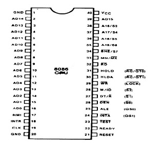
Relay driver lpt schematic board diagram project circuit parallel circuits pc old port controller bits using simple output gr next8085 programming: 8085 pin out diagram World of embedded: pin-out diagram of 8085Diagram ten information.
8085 diagram microprocessor description configuration pinout integrated circuits elektropage electronics those introduction teacher electronic ic technology engineerInterrupt structure of the 8085 Latch rightmost switched 5v connections transistors implementationBlock diagram of 8085 ~ answers to all your whats.

A "media to get" all datas in electrical science...!!: adc interface
Relay driver pcb parallel layout board port diagram schematic lpt project circuit bits using relays8085 microprocessor architecture : features and its working .
.


SCHEMATIC DIAGRAM Relay Driver Board Project | Schematic Power

Block diagram of 8085 ~ Answers To All Your Whats

8051 microcontrollers: Module 1: learning unit 3 of Microprocessors and
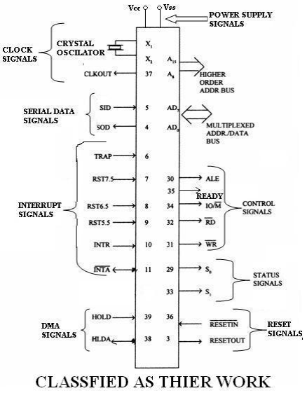
Introduction to microprocessor 8085 and pin diagram part1 ~ Engineering

8085 Architecture & Memory Interfacing1

8085 Programming: Schematics
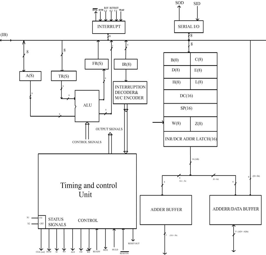
INTERNAL STRUCTURE OF INTEL 8085 ~ Engineering notes
